
Sentaurus Mesh
3. Using the Tensor-Product Mesh Generator
3.1 Overview
3.2 Basic Mesh Controls
3.3 Mesh Generation for EMW
3.4 Detecting Short Edges
3.5 Including Doping Information
Objectives
- To introduce the tensor-product mesh generation capabilities of Sentaurus Mesh.
3.1 Overview
The tensor-product meshes generated by Sentaurus Mesh are used primarily by Sentaurus Device Electromagnetic Wave Solver (EMW) and the TCAD to SPICE variability simulator, Garand.
To generate a tensor-product mesh using Sentaurus Mesh, you must specify the EnableTensor option in the IOControls section. Alternatively, you can use EnableSections in the IOControls section, which instructs Sentaurus Mesh to respect all specified sections. All the necessary controls for tensor-product mesh generation are specified in the Tensor section of the command file, which can include different subsections:
Tensor {
  Mesh {...}
  EMW {...}
}
where:
- The Mesh subsection defines the general tensor-grid controls.
- The EMW subsection defines dedicated controls for EMW applications.
For very large structures, you can speed up meshing by running Sentaurus Mesh in parallel. To do so, you can specify the number of threads in the IOControls section with numThreads=<integer>.
3.2 Basic Mesh Controls
The Mesh subsection defines the basic tensor-mesh controls, the most important of which will be introduced here. For more details, refer to the "Tensor Section" section, in Chapter 2, of the Sentaurus™ Mesh User Guide.
All the Sentaurus Mesh commands discussed in this section are contained in the Sentaurus Workbench project Applications_Library/GettingStarted/snmesh/TensorMesh. To work with the project, start Sentaurus Workbench and copy the project TensorMesh to a local directory within the Sentaurus Workbench working directory.
The command file is partitioned by the Sentaurus Workbench parameter example. To experiment with commands, add a new example in the Sentaurus Workbench project table, and add your commands in a new example section in the command file.
3.2.1 Default settings
Starting with an empty Mesh subsection (compare example=2), Sentaurus Mesh uses reasonable default values. The most important defaults are:
- maxCellSize: 10% of geometry in each direction
- grading: Switched on
For a dummy 2D CMOS image sensor (CIS) boundary, this results in a tensor mesh as shown in Figure 1 (left). Note the overall discretization of approximately 10 nodes in each direction due to the default value of maxCellSize and the clearly visible graded region around the top silicon interface.
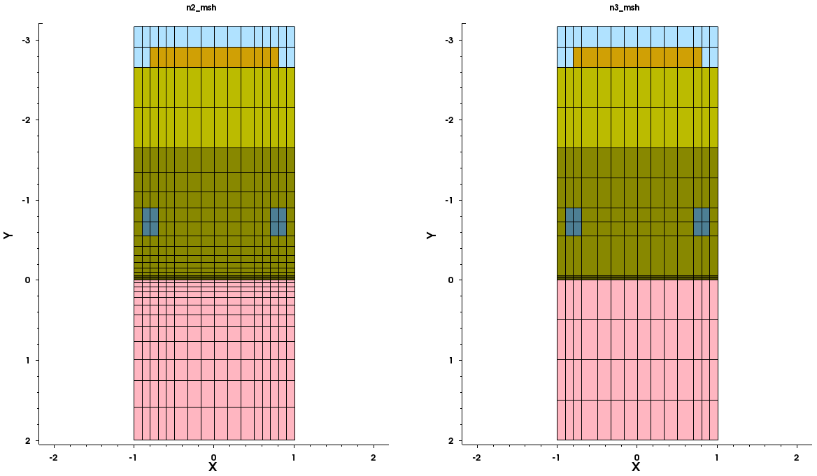
Figure 1. (Left) example=2 uses the default settings and (right) example=3 has grading switched off. (Click image for full-size view.)
3.2.2 Grading
By default, Sentaurus Mesh tries to create a smooth transition between cells of different element sizes. This is controlled by the keyword grading <grad>, where <grad> is a floating-point number specifying the maximum cell-size ratio of two adjacent elements. An individual grading factor can be specified for each direction using:
- grading = {<gradx> <grady>} for 2D structures
- grading = {<gradx> <grady> <gradz>} for 3D structures
To switch off grading, specify grading=off in the Mesh subsection (see Figure 1, right). Comparing the graded mesh (Figure 1, left) to it, additional horizontal lines are inserted in the top region of silicon due to the very small cells in the region on top of silicon. Similarly, vertical lines are added adjacent to the metal lines around x > –0.7 and x < 0.7.
3.2.3 Setting Cell Sizes
The size of tensor-grid elements in the bulk is a key parameter to be adjusted. As multiple refinements can be specified for a particular domain, you always specify an element size range with minCellSize and maxCellSize. Sentaurus Mesh tries to fullfill all of the specified requirements, however, it might not always be possible due to contradicting constraints or other limitations.
For example, with the following commands, you switch off grading and ensure that nowhere does the cell size drop below 0.01 μm, keeping the maximum cell size below 0.1 μm in each direction (see Figure 2, left).
    grading off
    minCellSize = 0.01
    maxCellSize = 0.1
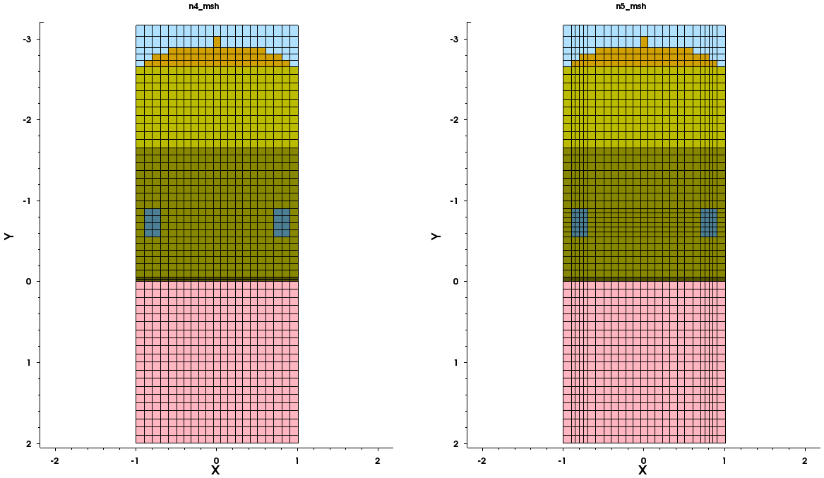
Figure 2. (Left) example=4 uses minCellSize and maxCellSize settings and (right) example=5 uses maxCellSize in silicon. (Click image for full-size view.)
3.2.4 Restricting Cell Size Refinements
Bulk refinements can be restricted to certain regions or materials and also to particular directions (see example=5). These local refinements overwrite global settings. Therefore, with the following line, the aluminum regions are refined more in the x- and y-directions (see Figure 2, right):
maxCellSize material "Aluminum" 0.01
However, looking more closely at the metal regions, you can see that the element size in the metal is approximately 0.05 μm and not 0.01 μm as actually requested, because the global minCellSize = 0.05 conflicts with maxCellSize=0.01 in the aluminum regions. The minCellSize requirements have a higher priority than the maxCellSize requirements. This ensures that a certain element size is not undercut, because the minimum cell size determines the time step in EMW simulations. This is why the final element size in metal is 0.05 μm, as defined by minCellSize.
Note that the minCellSize=0.05 setting also affects the thin region "M2" immediately above the silicon; it contains only one element in the y-direction instead of two as previously set.
With the following line, example=6 shows region- and direction-restricted refinement:
maxCellSize region direction "M6" "y" 0.02
This refines the lens "M6" in the y-direction (see Figure 3, left).
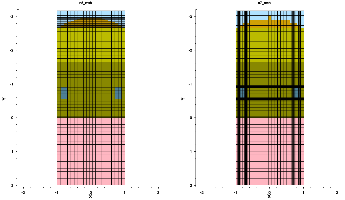
Figure 3. (Left) example=6 uses region- and direction-restricted refinement and (right) example=7 uses interface refinement. (Click image for full-size view.)
3.2.5 Interface Refinements
In addition to bulk refinement, the parameter maxBndCellSize offers interface (or boundary) refinement. In example=7, you use this parameter to refine the interfaces of the aluminum regions (see Figure 3, right):
maxBndCellSize interface material "Aluminum" "Insulator2" 0.01
Refinement occurs on both sides of the interface. A similar syntax can be used for region interfaces:
maxBndCellSize interface region "region1" "region2" 0.01
3.2.6 Refinement Windows
In addition to materialwise or regionwise refinements, Sentaurus Mesh offers the possibility to restrict refinements to user-defined rectangular windows. In example=8, the goal is to refine the photodiode area in the middle of the silicon bulk material (see Figure 4, left):
    window "PD" -0.5 0.5 0.2 0.5
    maxCellSize window direction "PD" "x" 0.05
    maxCellSize window direction "PD" "y" 0.02
You first define a window named "PD" with coordinates in the order <xmin> <xmax> <ymin> <ymax> (plus <zmin> <zmax> for 3D structures). Then, similar to region or material restriction, you use the parameter window to limit maxCellSize refinements to that window.
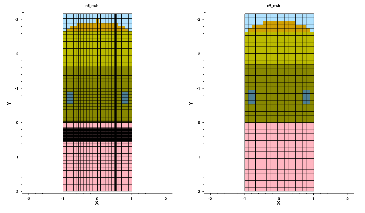
Figure 4. (Left) example=8 uses window-restricted refinement and (right) example=9 has an equidistant mesh. (Click image for full-size view.)
3.2.7 Equidistant Mesh
Sentaurus Mesh can also generate equidistant meshes by specifying the number of mesh points in each direction (see Figure 4, right):
    numPointsX = 20
    numPointsY = 50
The benefit of equidistant meshes is that generation is very fast. However, boundaries are adjusted to the equidistant grid. In this example, the size of the metal regions differs substantially, and the thin "M2" layer above the silicon is missing completely. Therefore, typically, these meshes are used for preliminary coarse estimates, or the element size must be chosen fine enough to minimize geometric errors.
3.3 Mesh Generation for EMW
Sentaurus Mesh allows the generation of tensor grids whose cell size depends on the optical path length of the incident light. In other words, you want to discretize the structure with a fixed number of points per wavelength. Such an approach is dedicated to the spatial mesh discretization suitable for Sentaurus Device Electromagnetic Wave Solver (EMW).
To run Sentaurus Mesh in EMW mode, you must use the EnableEMW option in the IOControls section. Alternatively, you can use EnableSections in the IOControls to instruct Sentaurus Mesh to respect all specified sections.
The tensor-mesh generation for EMW simulations is controlled in the EMW subsection in the Tensor section of the Sentaurus Mesh command file:
Tensor {
  EMW {...}
}
All the Sentaurus Mesh commands discussed in this section are contained in the Sentaurus Workbench project Applications_Library/GettingStarted/snmesh/TensorEMW. To work with the project, start Sentaurus Workbench and copy the project TensorEMW to a local directory within the Sentaurus Workbench working directory.
The command file is partitioned by the Sentaurus Workbench parameter example. To experiment with commands, add a new example in the Sentaurus Workbench project table, and add your commands in a new example section in the command file.
3.3.1 Setting the Complex Refractive Index
The complex refractive index (CRI) must be defined first with:
CRI WavelengthDep real imag
Similar to Sentaurus Device, you can instruct Sentaurus Mesh to use only the real part, or only the imaginary part, or both the real and imaginary parts for the optical path calculation by specifying the required parts. The effect on refinement is discussed here.
Similar to maxCellSize, the CRI model can be restricted to a certain region or material:
CRI material "Aluminum" WavelengthDep real
The CRI model constants are read from the ComplexRefractiveIndex sections of a Sentaurus Device parameter file. The file name can be set by the following command:
Parameter Filename = "@parameter@"
If no parameter file is defined, the defaults from Sentaurus Device are used. For convenience, a predefined Sentaurus Workbench parameter @parameter@ can be used to refer to a preprocessed version of the parameter file called snmesh.par.
Finally, to evaluate the CRI model and to calculate the n&k values, a wavelength in micrometers must be specified:
Wavelength = 0.6
The calculated n&k values for each region are reported in the log file:
refractive & kappa for each material using (n k) to set cell size:

-------------------------------------------------
material: Aluminum
M3a:   			(1.2 7.26)
M3b:   			(1.2 7.26)
...
3.3.2 NodePerWavelength Refinement
Similar to the maxCellSize refinement, the nodePerWavelength (or npw) refinement creates a maximum cell-size refinement. However, the actual value is calculated according to the wavelength and the CRI as follows:
- WavelengthDep Real:

- WavelengthDep Imag:

- WavelengthDep Real Imag:

As an example, using WavelengthDep Real, a wavelength of 0.5 μm, and a refractive index of 2.5 with npw=10, Sentaurus Mesh will place 10 nodes into the optical length of a wavelength, which corresponds to 0.2 μm in real space. Therefore, that the element size would be 0.02 μm.
Figure 5 (left) shows a simplistic case in example=2, with a very coarse mesh, typically used to quickly run EMW without expecting realistic results:
    CRI WavelengthDep real imag
    NPW = 5
Note how the y-refinement becomes progressively coarser from bottom to top as the refractive index decreases, from silicon with 3.939 to gas with 1.
The finer mesh inside the metal regions is obvious. This is because you switched on the imaginary refractive index part for the CRI, which has a large value of 7.26.
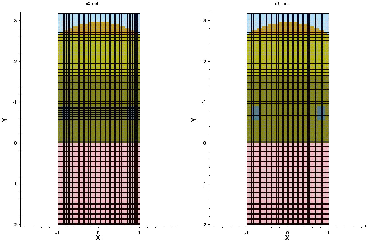
Figure 5. (Left) example=2 uses npw refinement with "CRI WavelengthDep real imag" everywhere and (right) example=3 uses "CRI real" for metal regions. (Click image for full-size view.)
In example=3 (see Figure 5, right), you switched off the imaginary part of the CRI. Therefore, the finer mesh in the metal regions disappears:
    CRI WavelengthDep real imag
    CRI material "Aluminum" WavelengthDep real
    NPW = 5
The npw refinements can be specified not only globally but also individually for each direction (see example=4, Figure 6, left):
    CRI WavelengthDep real
    NPWX = 5
    NPWY = 10
The element size in the y-direction is reduced in all regions.
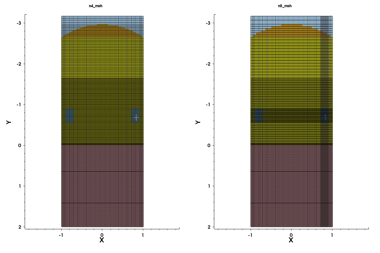
Figure 6. (Left) example=4 uses npwx and npwy separately, and (right) example=5 uses a materialwise npw setting. (Click image for full-size view.)
In addition, regionwise or materialwise as well as direction-limited specifications are possible:
npw material "materialName" <integer>
npw material direction "materialName" "x | y | z" <integer>
npw region "regionName"" <integer>
npw region direction "regionName" "x | y | z" <integer>
See example=5 in Figure 6 (right):
    CRI WavelengthDep real
    NPW = 5
    NPW region "M3a" 30
    NPW material direction "Silicon" "y" 10
All refinements are relaxed to 5 npw, and only the y-refinement in the silicon is kept at 10 npw. In addition, the right metal region has a very fine refinement of 30 npw.
3.3.3 Additional Options
Similar to the Mesh subsection previously described, the EMW subsection offers a grading parameter. By default, grading is switched on, but it can be switched off with grading off. Grading settings in the EMW subsection overwrite the grading settings in the Mesh subsection.
A single element layer is not well represented in EMW because the refractive indices are interpolated at the interfaces. Therefore, it is recommended to resolve a region with at least two cells in each direction. If an EMW subsection is present in the command file, by default, Sentaurus Mesh checks whether all layers are resolved with at least two elements. This check can be switched off by specifying NoEMWSolverConstraintsCheck in the EMW subsection.
3.4 Detecting Short Edges
For EMW simulations, the shortest edge length is critical for the maximum stable time step, which fundamentally determines the runtime. The stable time step is calculated using the Courant criteria and is proportional to the shortest edge length. Therefore, to achieve the maximum stable time step, short edges must be avoided.
To detect short edges, Sentaurus Mesh can report the minimum and maximum edge lengths in each coordinate direction, globally as well as for each region in the log file. To activate this report, specify verbosity=3 in the IOControls section of the command file.
For a simple structure, the report looks like:
________________________________________________________
# cells:                          464
# cells in X direction:           16
# cells in Y direction:           29
________________________________________________________
Max cell size in X direction:     0.166667
Min cell size in X direction:     0.1
Max cell size in Y direction:     0.5
Min cell size in Y direction:     0.025
________________________________________________________
Maximum grading in X direction:   1.66667
Maximum grading in Y direction:   1.96078
________________________________________________________
Region Name                            M1b
Material Name                          Silicon
# cells:                               54
Max cell size in X direction:          0.166667
Min cell size in X direction:          0.166667
Max cell size in Y direction:          0.231029
Min cell size in Y direction:          0.0387475
...
3.5 Including Doping Information
The tensor meshing scheme can be used with doping definitions as discussed in Section 2.8 Defining the Doping Profile. To incorporate doping into the mesh, call Sentaurus Mesh with the options -rect -gtdr, or run Sentaurus Mesh from within Sentaurus Workbench by right-clicking the Sentaurus Mesh tool icon and selecting Properties, and enter -rect -gtdr in the Command Line field.
The examples discussed here use a simple NMOS 2D device to demonstrate this capability. The example is contained in the Sentaurus Workbench project Applications_Library/GettingStarted/snmesh/TensorDoping.
The first experiment (example=2) defines some constant and analytic doping profiles as follows:
Definitions {
  Constant "substrate" {
    Species = "BoronActiveConcentration"
    Value = 1e+16
  }
  ...
}
and places this profile in a Placements section:
Placements {
  Constant "substrate" {
    Reference = "substrate"
    EvaluateWindow {
      Element = material ["Silicon"]
    }
  }
  ...
}
Figure 7 (left) shows the analytic doping profile.
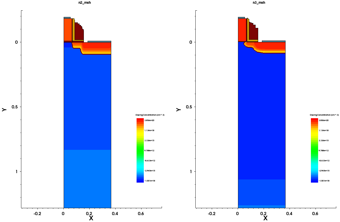
Figure 7. (Left) example=2 showing an analytic doping profile and (right) example=3 showing a submesh doping profile. (Click image for full-size view.)
Finally, an equidistant tensor mesh is defined:
}
Tensor {
  Mesh {
    numPointsX = 100
    numPointsY = 1000
  }
}
Figure 8 shows the final mesh.
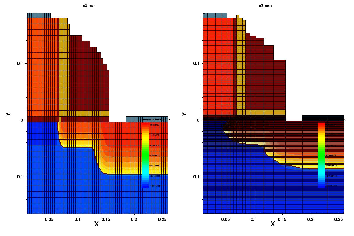
Figure 8. (Left) example=2 showing an analytic doping profile on an equidistant mesh and (right) example=3 showing a submesh doping profile using window refinements. (Click image for full-size view.)
The second experiment (example=3) incorporates the doping profile from an external TDR file:
Definitions {
  Submesh "doping" { Geofile = "doping_msh.tdr" }
}

Placements {
  Submesh "doping" { Reference = "doping"  }
}
Figure 8 (right) shows the doping profile. This time, a more sophisticated meshing strategy is applied using different, partially overlapping windows to resolve the channel and the drain more accurately:
Tensor {
  Mesh {
    minCellSize direction "x" 0.005
    maxCellSize = 0.05
    window "active" 0 0.365 -0.2 0.2
    maxCellSize window direction "active" "y" 0.005
    window "channel" 0 0.15 -0.005 0.05
    maxCellSize window direction "channel" "y" 0.001
    window "source" 0.1 0.365 0.0 0.14
    maxCellSize window direction "source" "y" 0.002
  }
}
For overlapping maxCellSize refinements, Sentaurus Mesh uses the smallest value in the overlapping domain.
Copyright © 2017 Synopsys, Inc. All rights reserved.