
Sentaurus Structure Editor
4. Generating Meshes
4.1 Overview
4.2 Defining Global Mesh Settings
4.3 Defining Regional Refinements
4.4 Saving the Model
4.5 Meshing the Device Structure
4.6 Assignment
Objectives
- To set up meshing strategies for 2D devices in Sentaurus Structure Editor.
4.1 Overview
This section provides instructions on how to control the mesh generation process.
This process is performed in two steps. The first step defines the meshing strategy, which includes the maximum and minimum meshing step definition in each device dimension as well as the mesh refinement strategies. The second step links the defined strategy from the first step to a specific target, which is, in general, a material, or a device region, or a user-defined evaluation window.
Different device regions have different roles in terms of determining the device performance, thereby the required meshing strategies for these regions are typically different.
4.2 Defining Global Mesh Settings
The first step always is the definition of mesh controls that are applied to the entire device structure.
For that, first you define the window, which covers the entire device domain:
- Switch off automatic region-naming by choosing Draw > Auto Region Naming.
- Switch on the Exact Coordinates mode by choosing Draw > Exact Coordinates or
click the
 toolbar button.
 - Choose Mesh > Define Ref/Eval Window > Rectangle.
In the view window, draw a rectangular window covering the entire device.
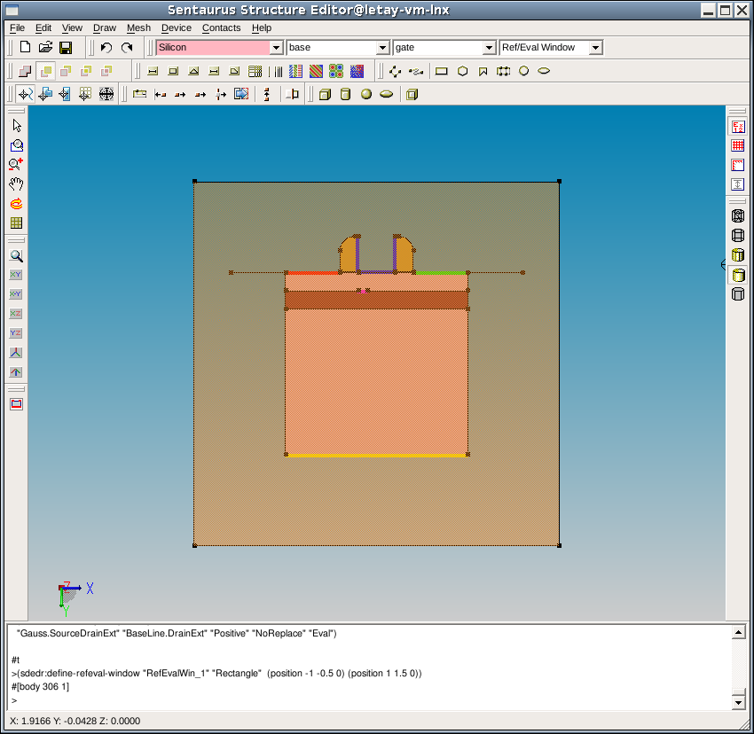
Figure 1. Refinement window covering the entire device. (Click image for full-size view.)
- In the Exact Coordinates dialog box, type (-1 -0.5) in the First Vertex fields, and type (1 1.5) in the Second Vertex fields.
- In the Ref/Eval Window Name field, type RefWin.all,
which will be referred to in the subsequent steps.
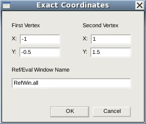
Figure 2. Exact Coordinates dialog box.
- Click OK.
The corresponding Scheme command is:
(sdedr:define-refeval-window "RefWin.all"
  "Rectangle" (position -1 -0.5 0) (position 1 1.5 0))
In the next step, you associate the global refinement window with the refinement box and select the mesh controls to be used globally:
- Choose Mesh > Refinement Placement.
The Refinement Specification dialog box is displayed.
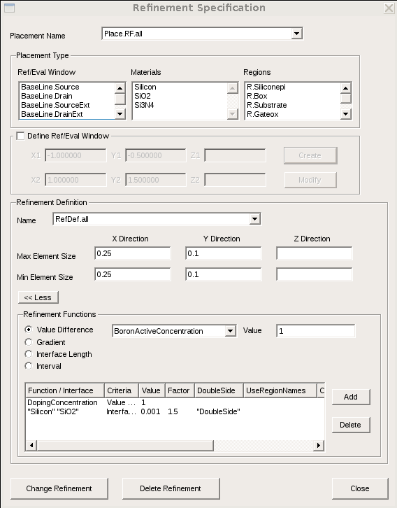
Figure 3. Refinement Specification dialog box for global refinement definition. (Click image for full-size view.)
- Type PlaceRF.all in the Placement Name field.
- Under Placement Type, in the Ref/Eval Window field,
select RefWin.all.
This selection associates the global refinement window with further settings applied in this dialog box. - Under Refinement Definition, type RefDef.all in the Name field. Then, enter the minimum and maximum mesh step values in both the x- and y-directions.
- Click the More >> button to expand the dialog box.
- Select the Value Difference option, and choose DopingConcentration
from the list of names in the corresponding box. Enter 1 as a value.
Click the Add button.
This adds the net doping field, which is computed during meshing, as a criterion for the mesh refinement. - Under Refinement Functions, select the Interface Length option,
and enter Silicon as the first selected material and SiO2 as the second material.
Enter 0.001 as a value and 1.5 as a factor.
Click Add.
This adds the silicon–SiO2 interface as a criterion for the mesh refinement at the interface. - Click Create Refinement if you enter it for the first time, or click Change Refinement for further refinement modifications.
- Click Close.
The corresponding Scheme commands are:
(sdedr:define-refinement-size "RefDef.all" 0.25 0.1 0.25 0.1)
(sdedr:define-refinement-placement "PlaceRF.all" "RefDef.all" "RefWin.all")
(sdedr:define-refinement-function "RefDef.all"
  "DopingConcentration" "MaxTransDiff" 1)
(sdedr:define-refinement-function "RefDef.all" "MaxLenInt" "Silicon" "Oxide"
  0.001 1.5 "DoubleSide")
4.3 Defining Regional Refinements
In addition to the global mesh refinement, the meshing strategy can be restricted to areas of interest, such as specific regions or restricted device domains.
In the discussed example, additional refinement is applied to the epi region R.Siliconepi and to the selected domain confined within the transistor channel.
To define a refinement box confined within the epi region R.Siliconepi:
- Choose Mesh > Refinement Placement.
The Refinement Specification dialog box is displayed.
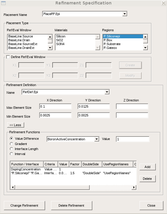
Figure 4. Refinement Specification dialog box for regionwise refinement specification. (Click image for full-size view.)
- Type PlaceRF.Epi in the Placement Name field.
- Under Placement Type, in the Regions field, select
R.Siliconepi.
This selection instructs the mesh engine to confine the refinement within the selected region. - Under Refinement Definition, type RefDef.Epi in the Name
field. Then, enter the minimum and maximum mesh step values in both the x- and y-directions.
The values used here are smaller than those used for the global mesh refinement definition. - Click the More >> button to expand the dialog box.
- Select the Value Difference option, and choose DopingConcentration
from the list of names in the corresponding field. Enter 1 as a value.
Click the Add button.
Due to the smaller minimal steps used here, compared to the global refinement settings, a finer mesh refinement on doping inside the epi region will be produced. - Under Refinement Functions, select the Interface Length option.
Select the UseRegionNames option, and enter R.Siliconepi as the first interface
region and R.Gateox as the second interface region.
This will apply the mesh refinement at the specified region interface only. - Select the DoubleSide option to instruct the mesh engine to refine the mesh on both sides of the interface.
- Enter 0.0002 as a value and 1.5 as a factor.
- Click Add.
The corresponding Scheme commands are:
(sdedr:define-refinement-size "RefDef.Epi" 0.1 0.0125 0.0025 0.0025)
(sdedr:define-refinement-function "RefDef.Epi"
  "DopingConcentration" "MaxTransDiff" 1)
(sdedr:define-refinement-region "PlaceRF.Epi" "RefDef.Epi" "R.Siliconepi")
(sdedr:define-refinement-function "RefDef.Epi" "MaxLenInt" "R.Siliconepi"
  "R.Gateox" 0.0002 1.5 "DoubleSide" "UseRegionNames")
The link between the refinement window and the refinement definitions can be directly set in the Refinement Specification dialog box. Here, you see how to refine the mesh in the middle of the transistor channel:
- Choose Mesh > Refinement Placement.
The Refinement Specification dialog box is displayed.
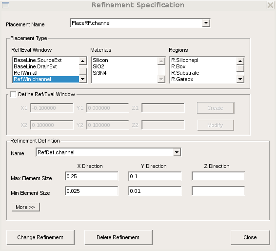
Figure 5. Refinement Specification dialog box for window-wise refinement specification. (Click image for full-size view.)
- Select the Define Ref/Eval Window option, and enter the minimum and maximum window coordinates of the refinement box.
- Click the Create button.
- Under Refinement Definition, type RefDef.channel in the
Name field. Then, enter the minimum and maximum mesh step values in both
the x- and y-directions.
The values used here are smaller than those used for the epi layer refinement definition. - Click Create Refinement.
You should see the refinement box highlighted in green after it is created.
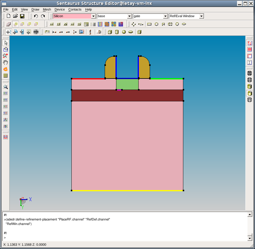
Figure 6. Window-based channel refinement box highlighted. (Click image for full-size view.)
The corresponding Scheme commands are:
(sdedr:define-refeval-window "RefWin.channel"
  "Rectangle" (position -0.1 0.0 0.0) (position 0.1  0.1 0.0))
(sdedr:define-refinement-size "RefDef.channel" 0.25 0.1 0.025 0.01)
(sdedr:define-refinement-placement "PlaceRF.channel" "RefDef.channel"
  "RefWin.channel")
4.4 Saving the Model
To save the model with the name soifet, follow the instructions in Section 2.12 Saving the Model.
The saved files are soifet.sat, soifet.scm, soifet_msh.cmd, and soifet_bnd.tdr.
Click to view all the commands discussed in this section in the command file soifet_dvs.cmd.
4.5 Meshing the Device Structure
To this point, several meshing strategies have been defined and placed in various device regions (windows). Now, you need to create the mesh in the device.
To build a mesh:
- Choose Mesh > Build Mesh.
The Build Mesh dialog box is displayed. - Enter soifet in the Save Grid to File field.
- Click Build Mesh.
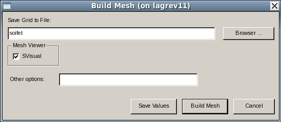
Figure 7. Build Mesh dialog box.
The corresponding Scheme command for launching the meshing operation is:
(sde:build-mesh "soifet")
This command saves two files used by Sentaurus Mesh, namely, the mesh command file soifet_msh.cmd and the TDR boundary representation soifet_bnd.tdr of the device. In the project, the n@node@ name is used instead of the soifet name.
Click to view the mesh command file soifet_msh.cmd.
Figure 8 shows the device structure with its current meshing and doping conditions, viewed using Sentaurus Visual.
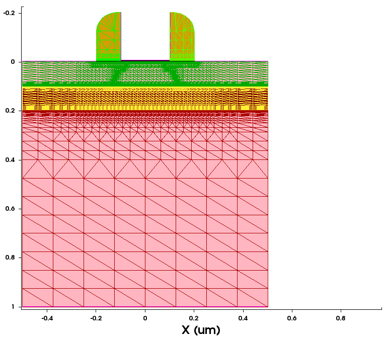
Figure 8. Two-dimensional SOI MOSFET meshed with above-described mesh controls.(Click image for full-size view.)
Figure 9 shows a detailed view of the mesh near the drain/channel junction region.
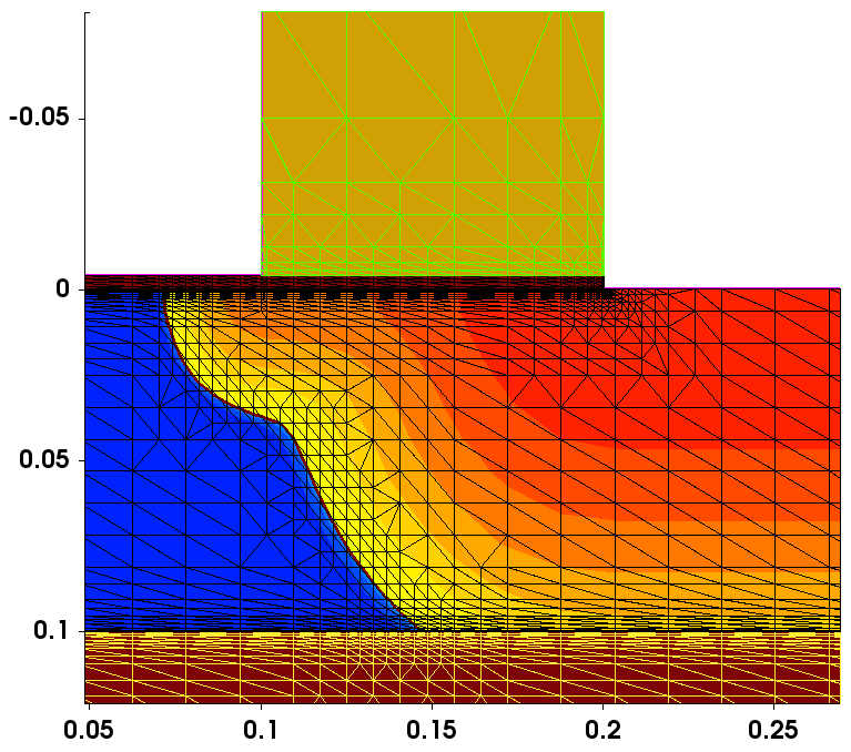
Figure 9. Mesh near the drain/channel junction region. (Click image for full-size view.)
Click to view all the commands discussed in this section in the command file soifet_dvs.cmd.
The complete project can be investigated from within Sentaurus Workbench in the directory Applications_Library/GettingStarted/sde/soifet.
4.6 Assignment
Define a meshing strategy for the SiGe HBT from Section 3.5 Assignment.
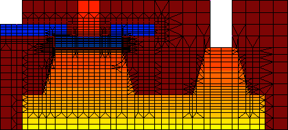
Figure 10. Two-dimensional SiGe HBT with its current meshing and doping conditions.
Click to view a solution of the command file sigehbt_dvs.cmd.
The complete project can be investigated from within Sentaurus Workbench in the directory Applications_Library/GettingStarted/sde/sigehbt.
Copyright © 2017 Synopsys, Inc. All rights reserved.