 main menu
| module menu
| << previous section
| next section >>
main menu
| module menu
| << previous section
| next section >>
Tool Overview
1. What Is TCAD?
1.1 TCAD and the Semiconductor Industry
1.2 Process Simulation
1.3 Device Simulation
Objectives
- To briefly introduce TCAD and who uses it.
1.1 TCAD and the Semiconductor Industry
Technology Computer-Aided Design (TCAD) refers to using computer simulations to develop and optimize semiconductor processing technologies and devices. TCAD simulation tools solve fundamental, physical, partial differential equations, such as diffusion and transport equations for discretized geometries, representing the silicon wafer or the layer system in a semiconductor device. This intensive physical approach gives TCAD simulation predictive accuracy.
Therefore, it is possible to substitute TCAD computer simulations for costly and time-consuming test wafer runs when developing and characterizing a new semiconductor device or technology.
TCAD simulations are used widely in the semiconductor industry. As technologies become more complex, the semiconductor industry relies increasingly more on TCAD to cut costs and speed up the research and development process. In addition, semiconductor manufacturers use TCAD for yield analysis, that is, monitoring, analyzing, and optimizing their IC process flows, as well as analyzing the impact of IC process variation.
TCAD consists of two main branches: process simulation and device simulation.
1.2 Process Simulation
In process simulation, processing steps such as etching, deposition, ion implantation, thermal annealing, and oxidation are simulated based on physical equations, which govern the respective processing steps. The simulated part of the silicon wafer is discretized (meshed) and represented as a finite-element structure (see Figure 1).
For example, in the simulation of thermal annealing, complex diffusion equations for each dopant species are solved on this mesh. For oxidation simulations, the growth of silicon oxide is simulated taking into account the oxygen diffusion, the mechanical stresses at corners, and so on.
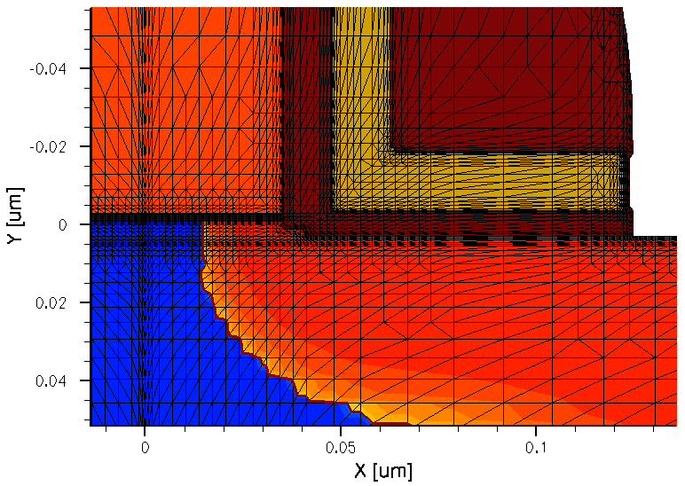
Figure 1. Magnification of gate-drain corner of an NMOSFET with finite-element grid. (Click image for full-size view.)
1.3 Device Simulation
Device simulations can be thought of as virtual measurements of the electrical behavior of a semiconductor device, such as a transistor or diode. The device is represented as a meshed finite-element structure. Each node of the device has properties associated with it, such as material type and doping concentration. For each node, the carrier concentration, the current densities, the electric field, the generation and recombination rates, and so on are computed (see Figure 2).
Electrodes are represented as areas on which boundary conditions, such as applied voltages, are imposed. The device simulator solves the Poisson equation and the carrier continuity equation (and possibly other equations). After solving these equations, the resulting electrical currents at the contacts are extracted (see Figure 3).
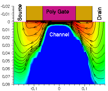
Figure 2. Current flow lines in a 0.13 μm NMOSFET at Vgs = 1.5 V and Vds = 3.0 V; shading represents current density.
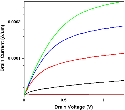
Figure 3. Drain current as a function of drain voltage for a 50 nm NMOSFET at Vgs = 0.25, 0.5, 0.75, 1.0, and 1.25 V.
main menu | module menu | << previous section | next section >>
Copyright © 2017 Synopsys, Inc. All rights reserved.